World-Class Manufacturing Infrastructure
Our facility houses a complete range of advanced PCB production equipment, from raw material preparation to final surface finishing.
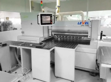
Laminate Cutting
High-precision CNC cutting of raw copper-clad laminates to panel size with ±0.1mm tolerance.
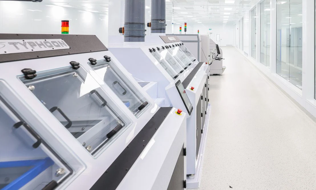
Drilling Center
Multi-spindle CNC drilling achieving 0.1mm mechanical holes and 0.075mm laser microvias.
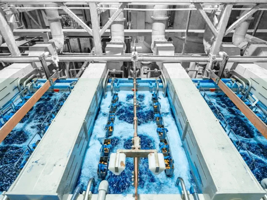
Plating Line
Automated electroless and electrolytic copper plating with automatic hoist for uniform deposition.
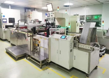
Plugging Lines
Vacuum resin filling of via holes for HDI boards, ensuring flat surface for fine-line patterning.
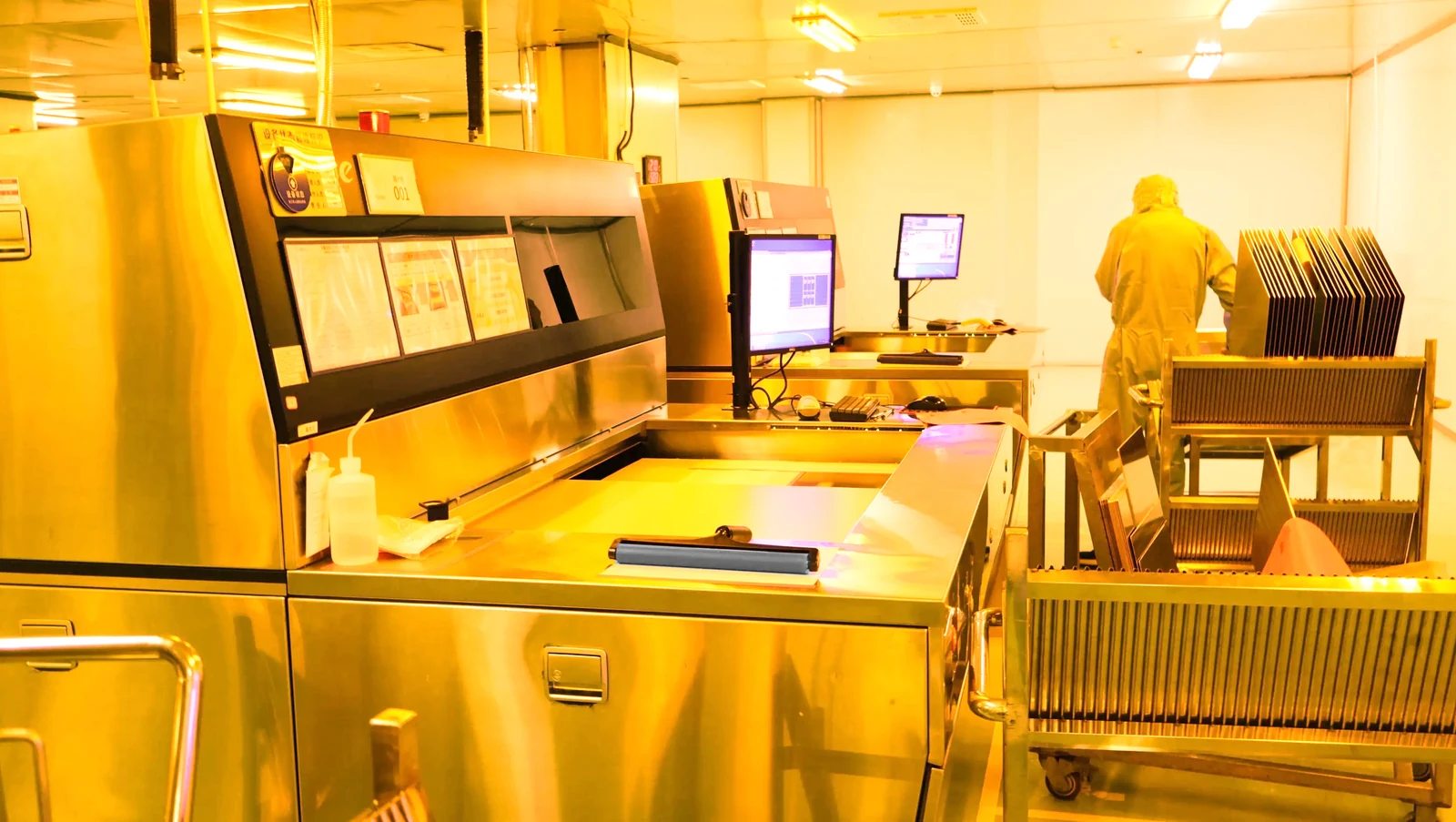
LDI Exposure
Laser Direct Imaging eliminates phototools, enabling 2mil/2mil trace/space with superior alignment.
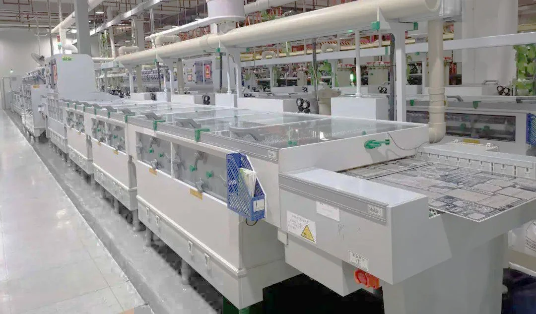
Etching Line
Horizontal spray etching with precise chemistry control for clean trace edges and minimal undercut.
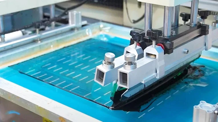
Silk Screen Lines
Automated solder mask and legend printing with 4mil minimum line width and multi-color capability.
Laminate Pressing
Vacuum hydraulic presses bond multilayer stacks with controlled temperature, pressure, and curing time.
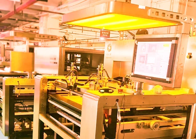
CCD S/M Exposure
CCD auto-alignment exposure machines ensure precise solder mask opening registration on every panel.
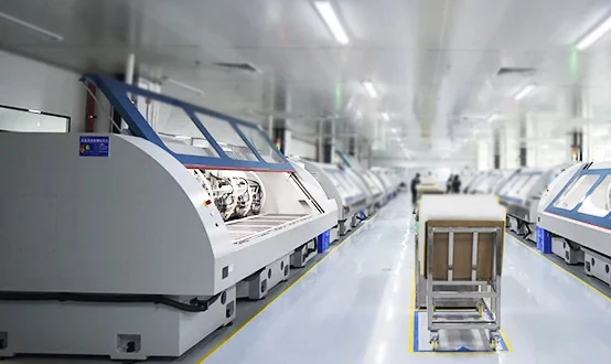
Routing
CNC routing and V-scoring machines depanel individual PCBs with ±0.05mm profile accuracy.
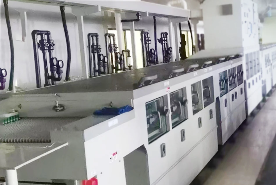
Surface Finishing
Complete surface finish workshop offering HASL, OSP, ENIG, immersion tin, and immersion silver for optimal solderability.
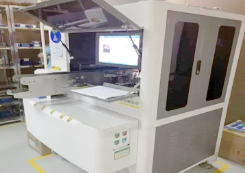
Grinding Driller
Brush deburring and oxide removal system ensures clean hole walls and optimal copper adhesion.