Comprehensive Testing & Inspection
Advanced inspection and testing capabilities ensuring the highest quality standards for every board we manufacture.

Film Checking
Dry film photoresist and artwork verification on illuminated light tables ensuring pattern accuracy before exposure.
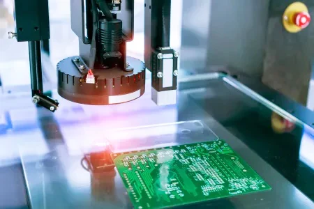
3D Checking
3D automated optical inspection detecting solder paste volume, component height, and coplanarity with micron-level precision.
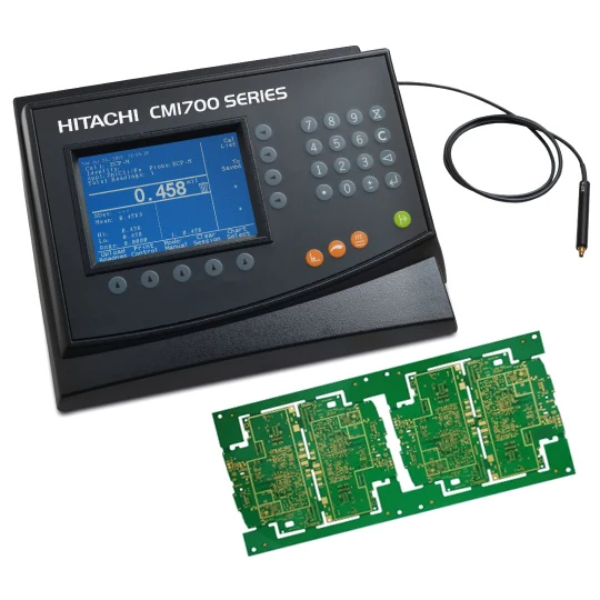
Copper Thickness Checking
Precision eddy-current and micro-resistance measurement ensuring copper clad laminate meets specified ounce requirements.
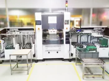
Electronic Testing
Comprehensive functional verification using oscilloscopes, multimeters, and custom test fixtures under real-world conditions.
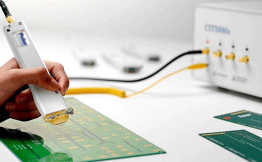
Impedance Testing
Time-domain reflectometry (TDR) and network analyzer measurement for controlled impedance traces and differential pairs.
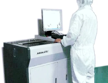
Ion Contamination Detecting
Ionic cleanliness testing per IPC-TM-650 2.3.25 to detect residual flux, salts, and contaminants that cause dendritic growth.
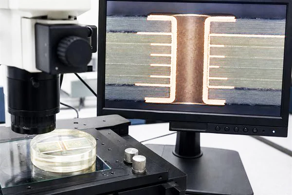
Microsection Analysis
Cross-sectional metallographic examination of plated through-holes, vias, and solder joints per IPC-TM-650 standards.
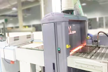
On Line AOI
In-line automated optical inspection integrated directly into the SMT production line for real-time defect detection.
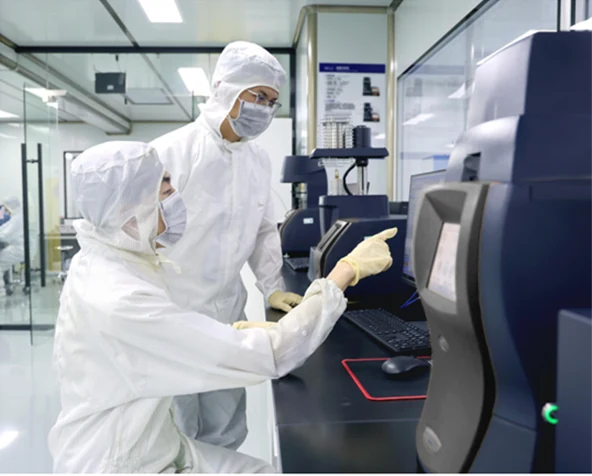
Quality Control Laboratory
Dedicated QC lab equipped with precision instruments for dimensional, electrical, and environmental testing.
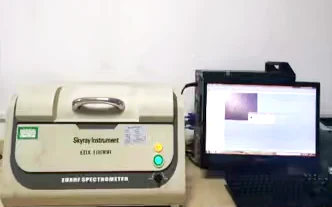
RoHS Checking
XRF screening and wet chemistry analysis verifying compliance with RoHS directive for lead-free and restricted substances.
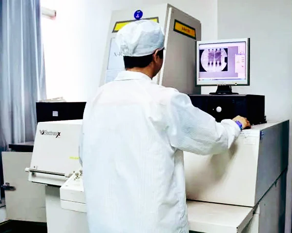
X-Ray Checking
Real-time X-ray analysis for BGA, QFN, and hidden solder joint verification without physical disassembly.
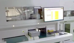
AVI Auto Inspecting
Automatic Visual Inspection system detecting scratches, foreign material, missing solder, and pad contamination at high speed.