From a bold vision to a global force in advanced PCB manufacturing — discover the story, purpose, and people behind Primo PCB.
The name Primo carries the meaning of "first," "foremost," and "of the highest quality." It is the standard we set for ourselves every single day. Primo PCB was founded in 2009 with a clear purpose: to become the first-choice partner for engineers and enterprises worldwide who refuse to compromise on quality, speed, or precision.
We believe that every electronic innovation — whether it is an electric vehicle powertrain, a life-saving medical device, or a 5G base station — begins with a single, perfectly engineered circuit board. Our mission is to make that first step flawless.
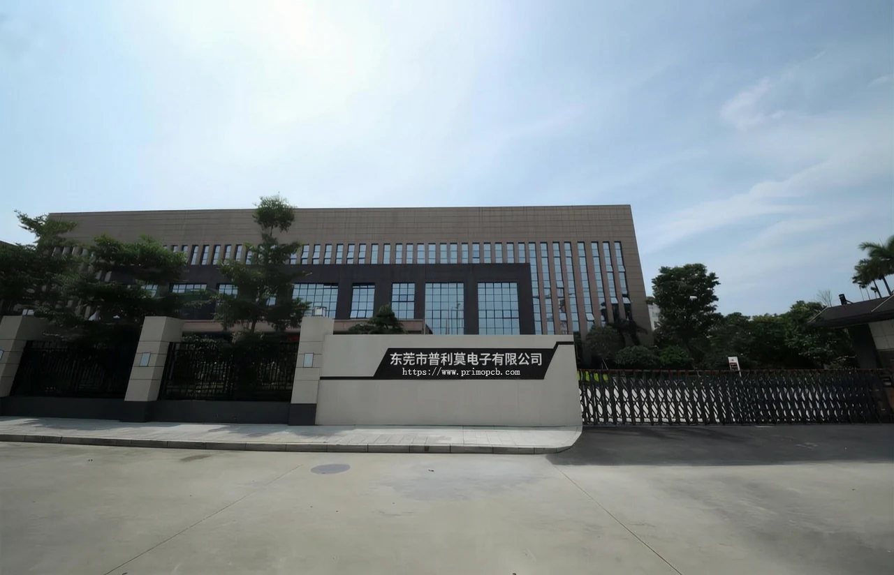
Headquartered in Dongguan, China, Primo PCB operates two state-of-the-art facilities spanning 50,000 square meters. With 800+ employees, including 120 R&D engineers, we have delivered over 10,000 projects to customers across 40+ countries, maintaining a 98.5% on-time delivery rate and a first-pass yield of 99.5%.
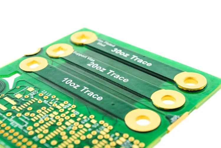
From 2-layer prototypes to 40-layer HDI boards, from rigid-flex to heavy-copper power PCBs, we combine cutting-edge equipment with obsessive quality control to turn your most complex designs into reliable reality.
A timeline of growth, investment, and relentless pursuit of excellence.
Primo PCB was established in Dongguan with a single production line and a team of 30 engineers, focused on delivering premium multilayer boards to local electronics manufacturers.
Expanded to international markets across Europe and North America. Achieved ISO 9001 and ISO 14001 certifications, establishing a quality-first culture that defines our operations today.
Invested in HDI laser drilling, automated optical inspection (AOI), and 12 high-speed SMT lines. Launched rigid-flex and metal-core PCB capabilities for automotive and medical sectors.
Deployed a full MES (Manufacturing Execution System) for real-time production traceability. Achieved IATF 16949 certification, opening doors to Tier-1 automotive OEM partnerships.
Opened a second 25,000 sqm facility dedicated to high-volume production. Daily output capacity reached 10,000 sqm, with support for up to 100-layer boards and 2mil/2mil trace/space.
Leading R&D in next-gen substrate technologies for AI accelerators and quantum computing. Committed to carbon-neutral manufacturing by 2035 as part of our sustainable growth roadmap.
The principles that guide every decision we make, from the factory floor to the boardroom.
To be the world's most trusted partner for advanced PCB manufacturing, enabling the next generation of electronic innovation through precision engineering, sustainable practices, and uncompromising quality.
Four pillars that define who we are and how we work with every customer, every day.
A glimpse into the facilities, teams, and moments that power our mission.
Modern production campus in Dongguan's high-tech industrial zone.
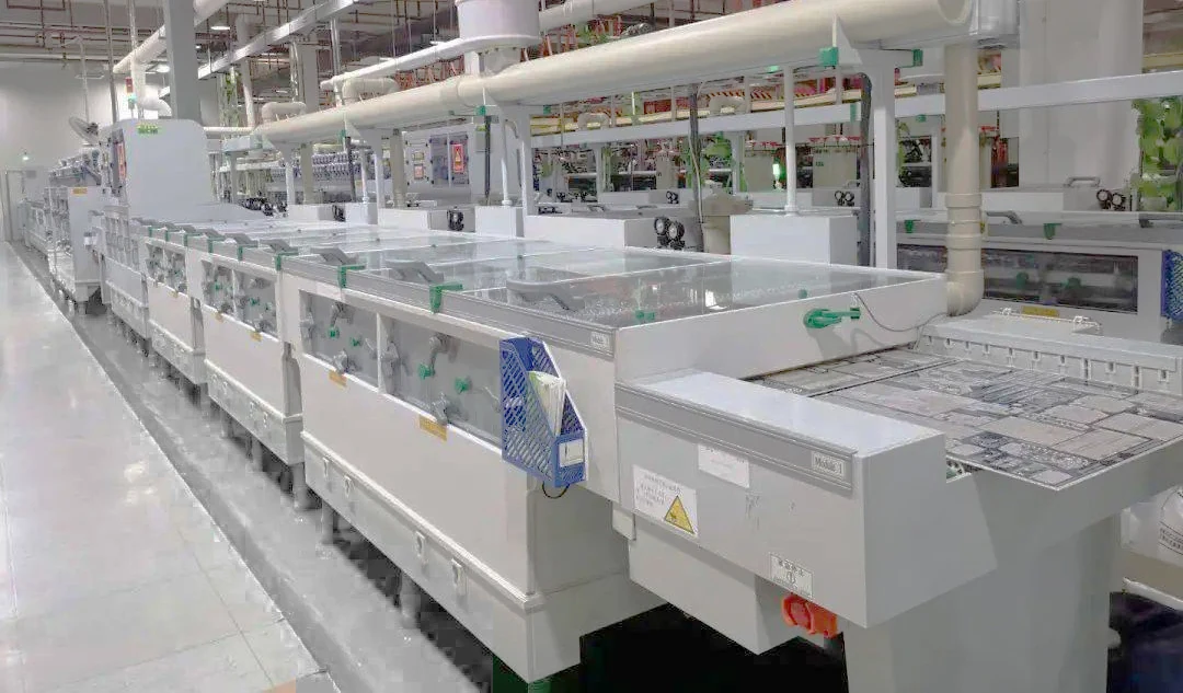
High-density interconnect boards under automated etching and plating lines.
Our 120-person R&D team reviews stack-ups and impedance simulations daily.
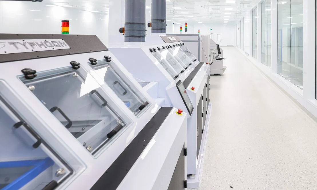
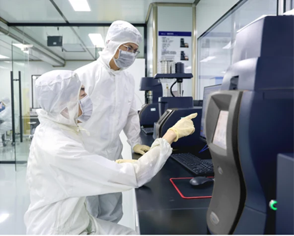
Controlled environment ensuring particle-free fabrication for medical and aerospace boards.
AOI, X-ray, and 4-wire Kelvin testing stations for 100% verification.
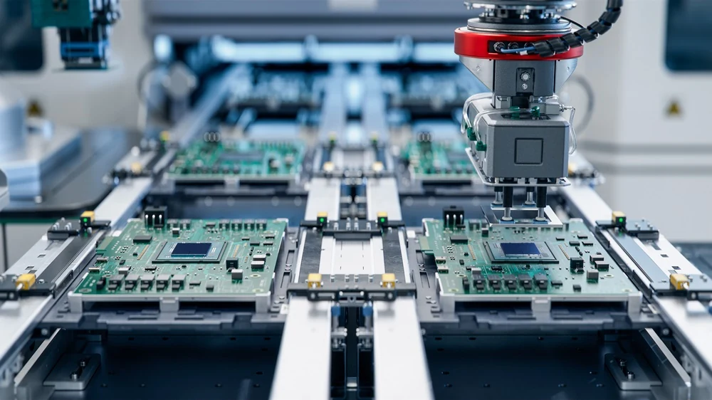
Robotic SMT placement with sub-millimeter accuracy for 01005 components.
Experience the difference that a first-class manufacturing partner makes. Get a free quote and DFM review within 24 hours.